As the data center ecosystem rapidly transitions toward Co-Packaged Optics (CPO) and Optical I/O (OIO) to meet the unprecedented demands of AI-driven bandwidth, several key technical and manufacturing challenges stand in the way of commercialization. These challenges are not merely theoretical; they are deeply intertwined with cost, energy efficiency, physical form factor, and silicon photonics manufacturing scalability!
At the 2025 TSMC North America Technology Symposium, the key points regarding silicon photonics remained consistent with the concepts we previously discussed in our articles. However, we also conducted a deeper analysis of TSMC’s silicon photonics progress presented at OFC50. In the future, we plan to further explore emerging companies and critical players in the silicon photonics supply chain, such as NewPhotonic, Lightwave Logic, ficonTEC, SURUGA SEIKI, Ayar Labs, RANOVUS ,Lightmatter, and Celestial AI.
We will also examine topics like CPO light sources using quantum dots, Quintessent’s innovations, and the future integration of silicon photonics with glass materials. These areas are all worthy of in-depth discussion.
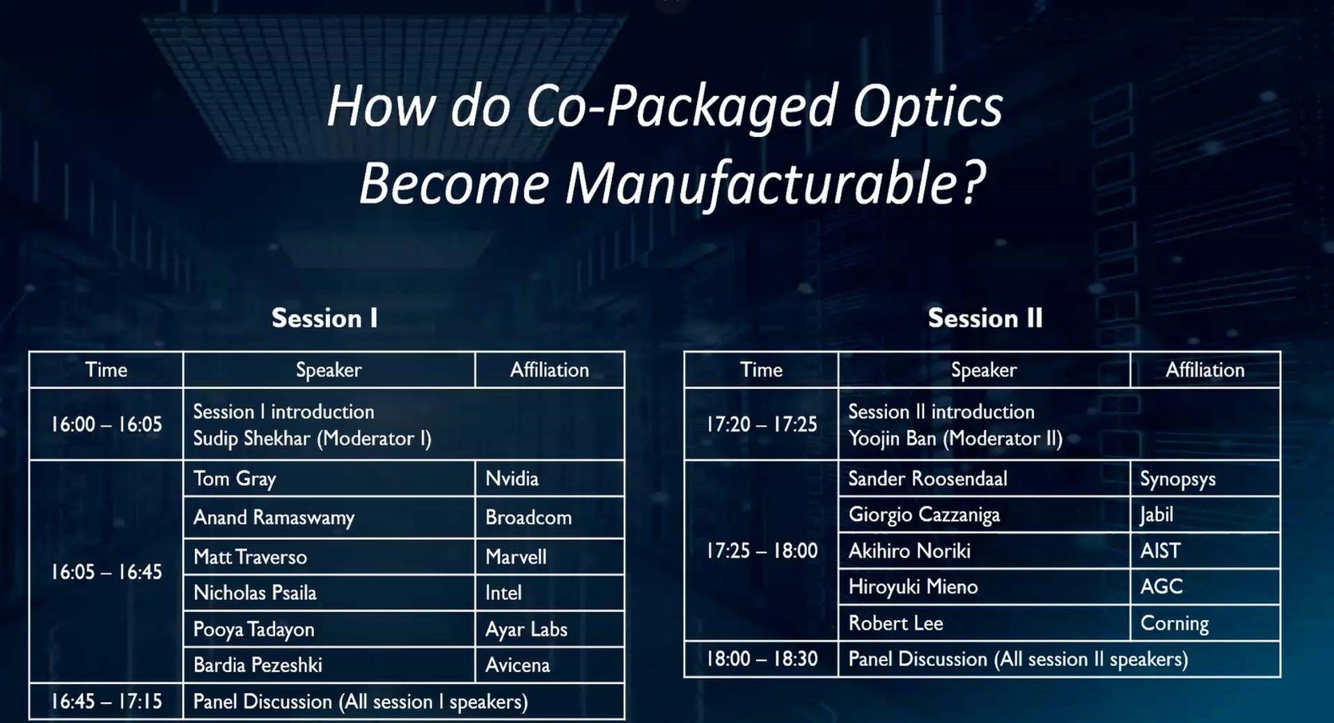
This conference featured in-depth discussions with participation from many leading companies across the industry. One of the core topics addressed was how to scale up Co-Packaged Optics (CPO) and achieve mass production readiness. This challenge inevitably ties back to the maturity and flexibility of TSMC’s silicon photonics platform.
A thorough understanding of the silicon photonics manufacturing flow is essential—especially given the high degree of customization among products from major players such as NVIDIA, Marvell, Broadcom, Cisco, NTT, MediaTek, Ranovus, AMD, Intel , IBM and others. Each company has taken a different path in developing their own CPO technologies.
Another key discussion point centered on the evolving direction of PIC (Photonic Integrated Circuit) design—moving toward higher bandwidth density and increased fiber count. However, this ambition introduces substantial technical hurdles. One major concern is how NVIDIA’s future AI chip, Feynman, will integrate optical engines. The implementation of optical interposers, especially the waveguide structure, remains a complex technical challenge.
Additionally, as we previously mentioned, silicon photonic products are highly customized by nature. Establishing a robust and reusable PDK (Process Design Kit) and ADK (Package Assembly Design Kits) will be critical in moving toward a standardized platform. This standardization could serve as a foundation for scalability.
Finally, thermal budget management is another vital issue. If not properly addressed, it can severely impact the overall optical performance and reliability of integrated photonic systems.
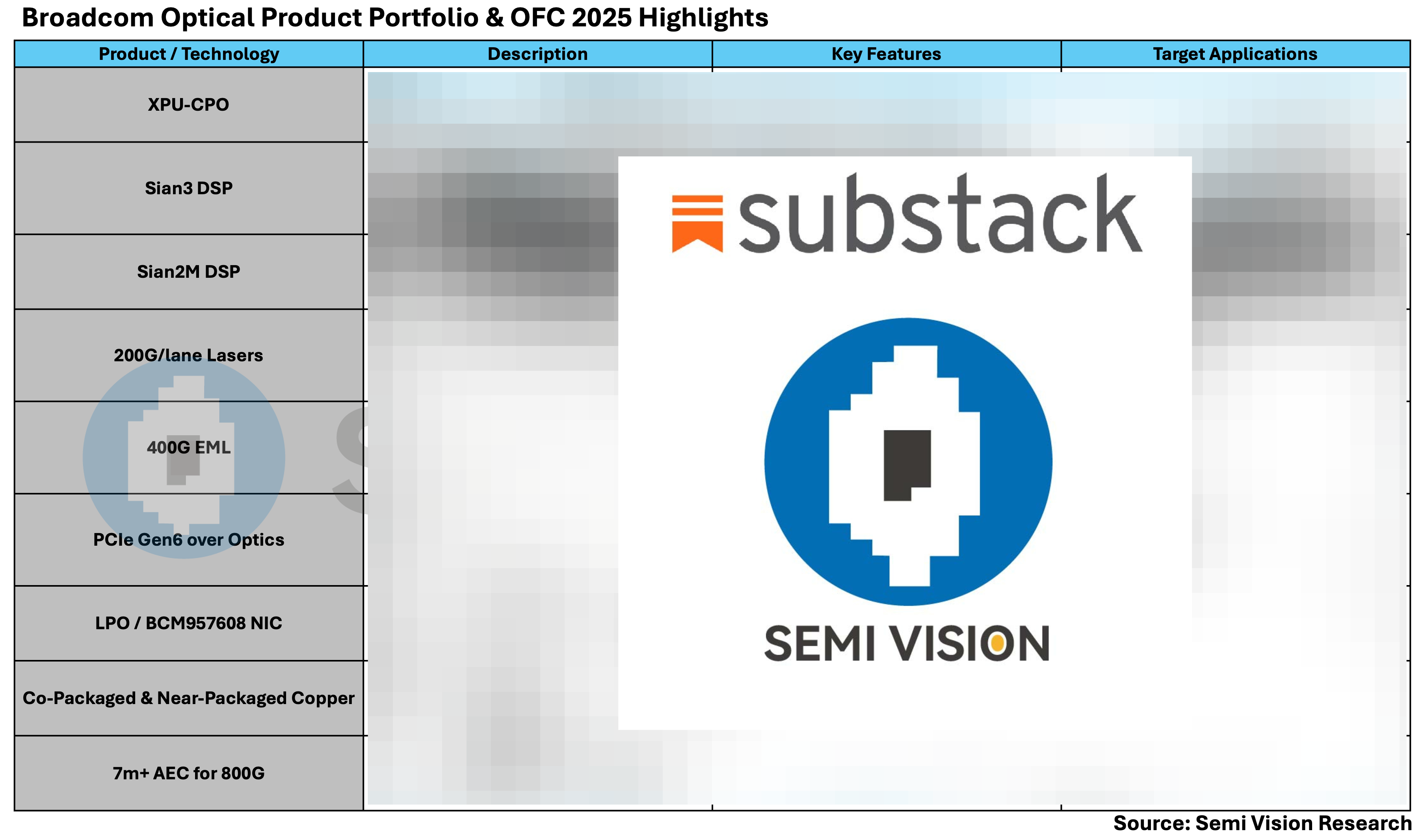
SemiVision will provide in-depth discussions on Nvidia, Broadcom, and Marvell, covering their strategies, technologies, and ecosystem developments in the optical and semiconductor domains.
NVIDIA is playing a key role in ushering in the era of silicon photonics, actively pushing its transition from research to large-scale commercialization.
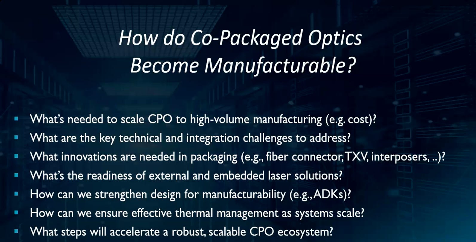
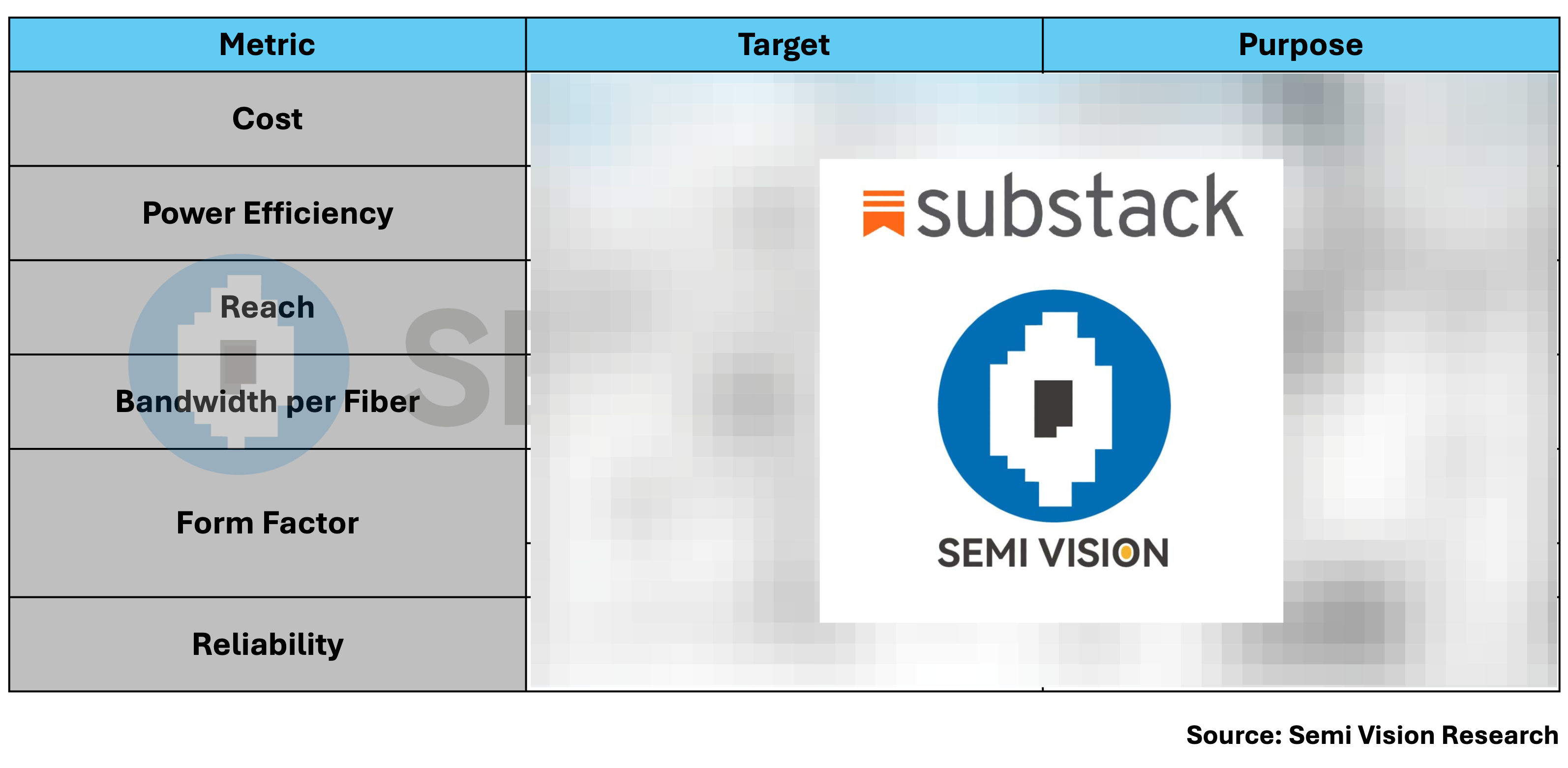
Key Commercialization Challenges for CPO Platforms
To make CPO manufacturable at scale, the solution must simultaneously meet the following constraints:
If you would like to explore the silicon photonics roadmaps of TSMC and NVIDIA in greater depth, please refer to our previously published articles for more detailed analysis and insights.
How TSMC’s Silicon Photonics Could Impact NVIDIA’s Future
2025 GTC Review: The Silicon Photonics Era Has Arrived – Get Ready!
NVIDIA x TSMC: A Milestone in Silicon Photonics and Optical Integration
Nvidia GTC AI Conference Preview: GB300, CPO switches, and NVL288
TSMC and NVIDIA Pioneering the Future of AI with Silicon Photonics Technology
CPO Switch Technology Analysis
How to Distinguish Between CPO and OIO? What Is Their Fundamental Difference?
How TSMC’s Silicon Photonics Could Impact NVIDIA’s Future
UMC’s Strength in the Silicon Photonics Supply Chain
Silicon Photonics Supply Chain – Opportunities and Challenges for Taiwan’s Supply Chain
Foxconn Research Institute:SiliconPhotonic Viewpoint _Opportunity and Challenges
Currently, NVIDIA plays the role of the system architect and PIC designer, especially for Optical I/O modules aimed at its future scale-out AI platforms. However, the actual silicon photonic manufacturing—particularly the modulators and photodetectors—is still handled by foundries, with TSMC being the primary manufacturing partner.
The reason? Making CPO manufacturable is not just a matter of layout and integration — it requires deep lithographic tuning and process-specific know-how that only select foundries possess. In particular:
Silicon Mach-Zehnder Modulators (MZMs) or Ring Resonator-based modulators must be finely tuned in the sub-wavelength regime, often relying on lithographic precision, implant profile control, and optical confinement techniques.
These structures are extremely sensitive to phase error, sidewall roughness, and alignment with the CMOS backend, which means that design portability between foundries is nearly impossible.
Foundries like TSMC, UMC, and GlobalFoundries possess unique device libraries, photonic PDKs, and in-house process calibrations that effectively form a proprietary optical process moat.
PIC designers must therefore co-develop with the foundry, often requiring multi-quarter tapeout/test/iteration cycles to reach commercial viability.
For TSMC’s concept of silicon photonics in 2025, you may refer to the following articles:
CPO Development statute updated (AMD (Ranovus), Broadcom, Cisco, IBM, Intel, and Marvell)
Silicon Photonics Manufacturing Process
Photolithography to optical device (PIC)
Automated Testing & Reliability(PIC + EIC)
The Rise of Photonic AI: TSMC’s SiN Technology Empowers NVIDIA’s Optical Ambitions
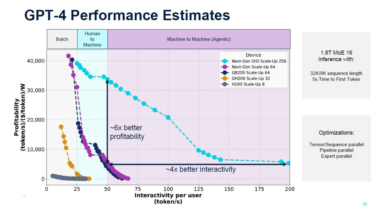
The chart illustrates that an eight-way H100 node, while adequate for batch-mode generative AI workloads, struggles with real-time human-to-machine interaction. Moving up to a 32-way GH200 configuration—equipped with 141 GB of HBM3E—brings noticeable gains in both cost-efficiency and performance.
A 64-GPU GB200 setup further enhances the performance curve, showing improved profitability and interactivity, but the difference between this and a similarly scaled future-generation Rubin (electrical I/O) system remains modest.
However, the real breakthrough emerges with Rubin architecture utilizing optical I/O instead of traditional electrical NVLink and NVSwitch connections. This innovation enables scaling to 256 coherent GPUs—something previously unachievable due to the physical limitations of copper cabling. With this optical infrastructure, machine-to-machine (agentic) multimodal processing becomes viable at scale.
As the chart shows, the Next-Gen OIO (optical I/O) Scale-Up 256 configuration dramatically outperforms all others, delivering up to ~6x better profitability and ~4x better interactivity compared to current state-of-the-art setups. This level of efficiency marks a transformative shift for large-scale AI inference.
The results validate a key design principle: avoid traditional networking bottlenecks; optical fabric like TeraPHY is the path forward.
As CPO systems move toward integration with electrical switch ASICs (e.g., Broadcom Tomahawk, Marvell Teralynx), the role of foundries becomes even more critical. Not just as wafer fabricators, but as platform-level enablers of:
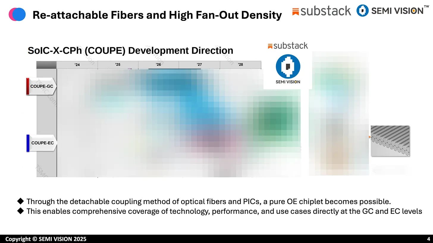
Heterogeneous Integration (e.g., SOIC, COUPE)
Thermal budget induced co-packaging optics reliability.
Photonic wafer-level testing and yield screening —> TSMC is ramping up investments in optical testing infrastructure in response to the increasing demand for Optical Engine manufacturing. According to SemiVision Research, TSMC has recently acquired a significant number of advanced Optical and electrical properties and testing systems from OOO and other global vendors.
Silicon + InP hybrid bonding (for lasers)
Photonic device reticle stitching across large dies —> Advanced Package Issue
TSMC’s silicon photonics roadmap, as discussed in SemiVision Research’s earlier reports, is focused on scaling:
High-speed modulator performance (>50 GHz)
Integration density (ring vs MZI-based layouts)
Thermal compensation mechanisms
Wafer-level photonic testing
Integration with front-end CMOS drivers and TIAs
This ecosystem is tightly coupled with Nvidia, Broadcom, Marvell, and other system vendors looking to bring CPO and OIO to production within the next 2–3 years.
The question “How does CPO become manufacturable?” is less about whether the technology works and more about who can scale it at data center volumes with consistent performance, reliability, and cost structure.
CPO success depends on:
Foundry-PIC designer collaboration
Deep device-level process control
High-yielding passive/active optical elements
Full-stack packaging and thermal management
Vendor-specific tuning within each foundry’s photonics platform
CPO is not a standalone module — it is a vertically integrated platform. And in this platform, foundries are no longer background players — they are at the heart of enabling AI’s optical future.
TSMC’s silicon photonic platform adopts a micro-ring-based design
Why Not Use a Multi-Wavelength Design?
NVIDIA has chosen a single-wavelength architecture, in contrast to Broadcom’s MZM-based multi-wavelength approach. The primary reason lies in the requirements of high-radix applications, which enable the construction of larger-scale networks and help reduce overall costs.
Whether NVIDIA will introduce a multi-wavelength version in the future remains to be seen and will largely depend on market demand.
Broadcom is currently utilizing a Mach-Zehnder Modulator (MZM)-based process, in combination with the FR4 electrical interface standard. The rationale behind this design choice was discussed in detail in our previous articles and will not be elaborated further here.
In contrast, Nvidia has adopted the DR4 optical module specification for its current deployments. However, according to insights from SemiVision Research, future CPO-based DWDM applications, particularly in MRM (Mid-Reach Module) systems, will require more diverse photonic integration strategies.
Both MZM and MRM-oriented designs are now being actively supported by TSMC’s silicon photonics platform, which offers differentiated solutions for various modulator types and channel densities.
For more detailed technical discussion and solution roadmaps, feel free to contact us directly for consultation.
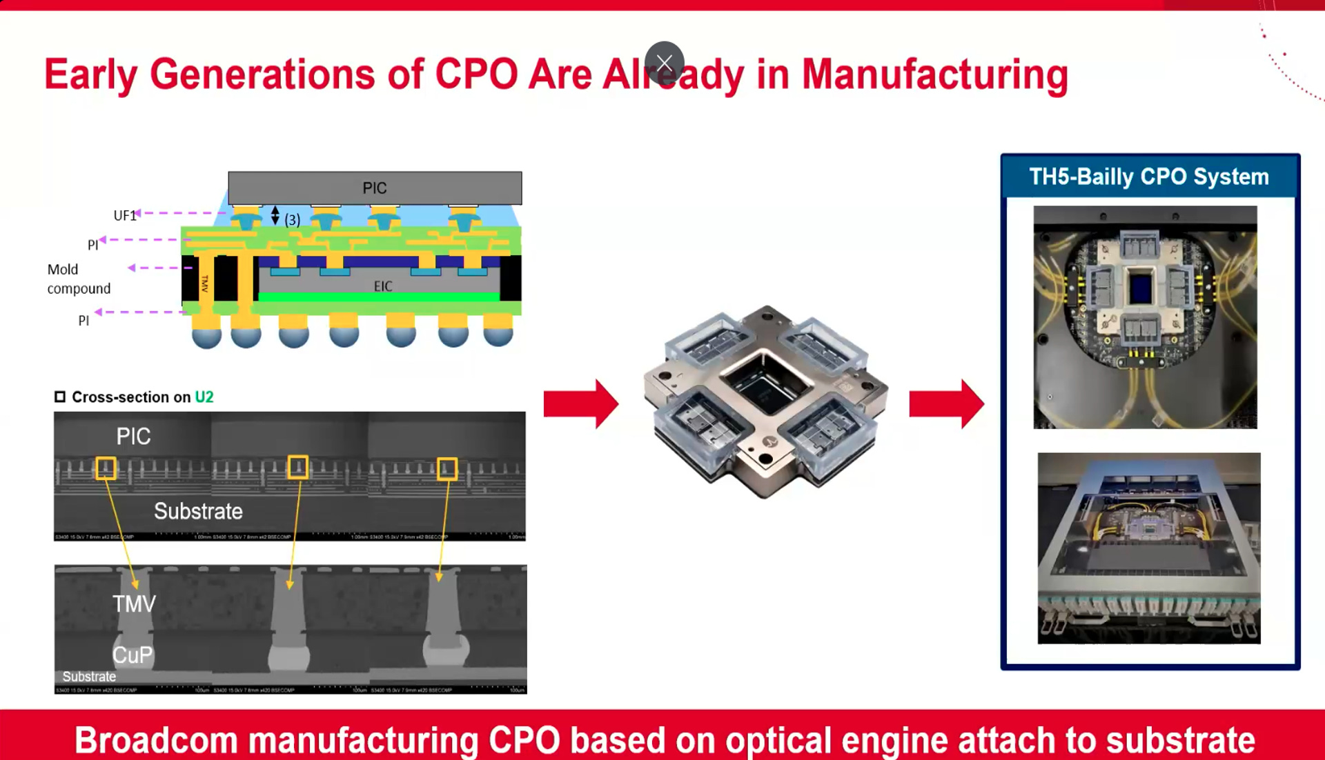
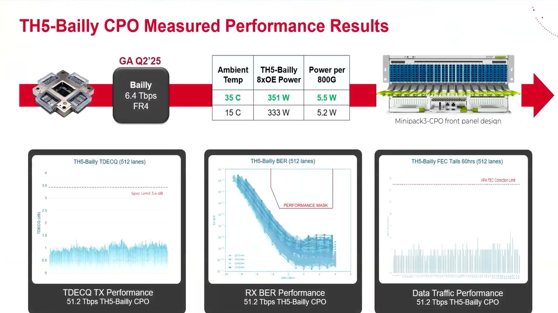
Broadcom’s early-generation Co-Packaged Optics (CPO) architecture adopted a distributed packaging approach, where key photonic and electronic components were fabricated and assembled separately. Specifically, Broadcom leveraged Wafer-Level Fan-Out (WL-FO) packaging technology, in which the Photonic Integrated Circuit (PIC) and the Electronic Integrated Circuit (EIC) were sourced from different foundry or fab partners (OO&OO).
The advanced packaging process itself was handled by Siliconware Precision Industries (SPIL), utilizing Redistribution Layer (RDL) technology to interconnect and integrate the components.
However, this approach brings significant challenges — particularly in the quality and uniformity of the RDL’s polyimide (PI) layer, which has a direct impact on both Signal Integrity (SI) and Power Integrity (PI). In high-speed optical-electrical systems like CPO, any variation or defect in the RDL stack-up can lead to timing jitter, impedance mismatch, or power noise, making RDL reliability a critical bottleneck for performance and scalability.
Broadcom’s Strategic Expansion in ASIC Services
Broadcom is actively expanding its presence in the ASIC (Application-Specific Integrated Circuit) services sector, playing a pivotal role in the AI infrastructure landscape. According to SemiVision Research, Broadcom’s key clients include major hyperscalers such as Google, Meta, and OpenAI. These collaborations involve the development of custom AI chips tailored to specific workloads, highlighting Broadcom’s commitment to delivering specialized solutions.
Notably, Broadcom has recently secured additional clients, including OpenAI and another undisclosed major player, further solidifying its position in the market. The company projects that its AI-related business with its top three hyperscaler clients could generate between $OO billion and $OO billion over the next two years .
If you’re interested in gaining deeper insights into Broadcom’s ASIC services and its client engagements, please feel free to reach out to us.
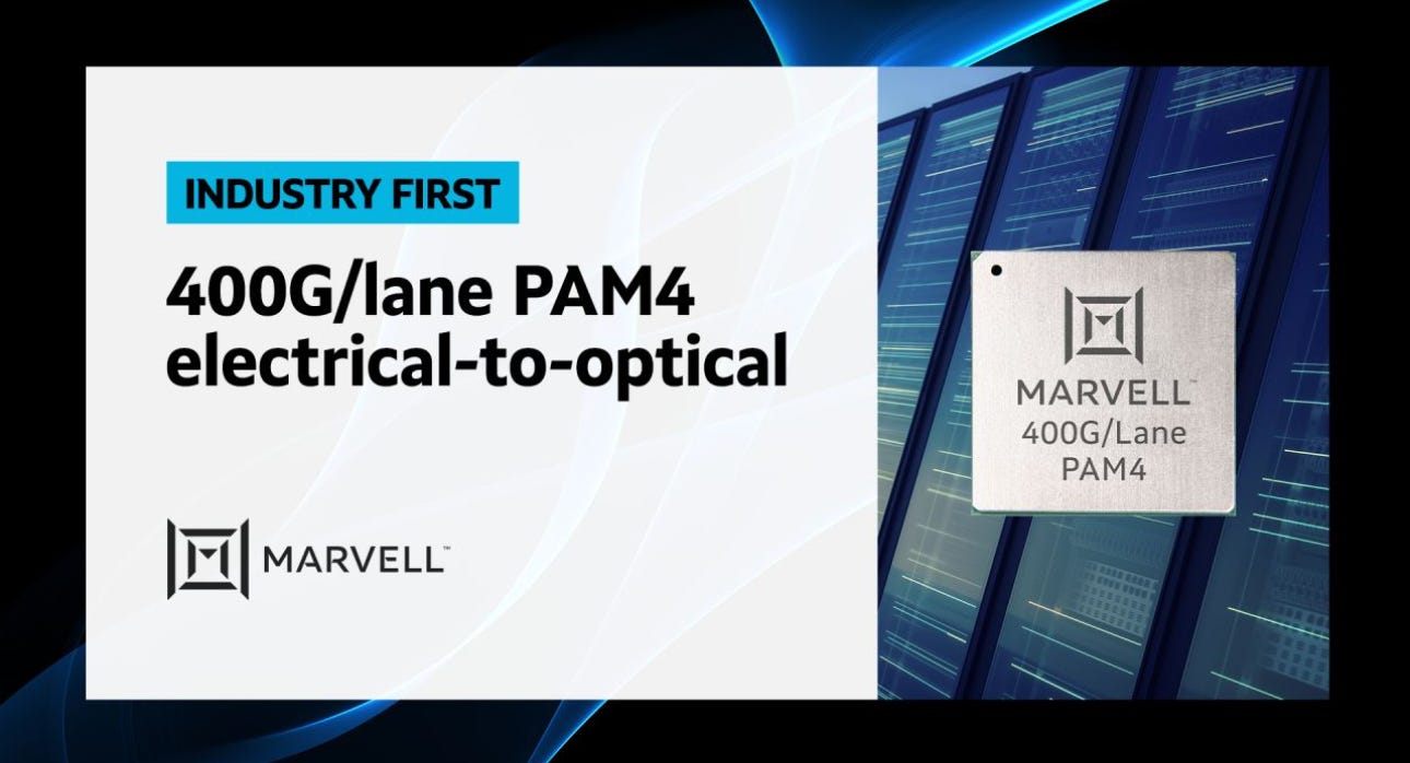
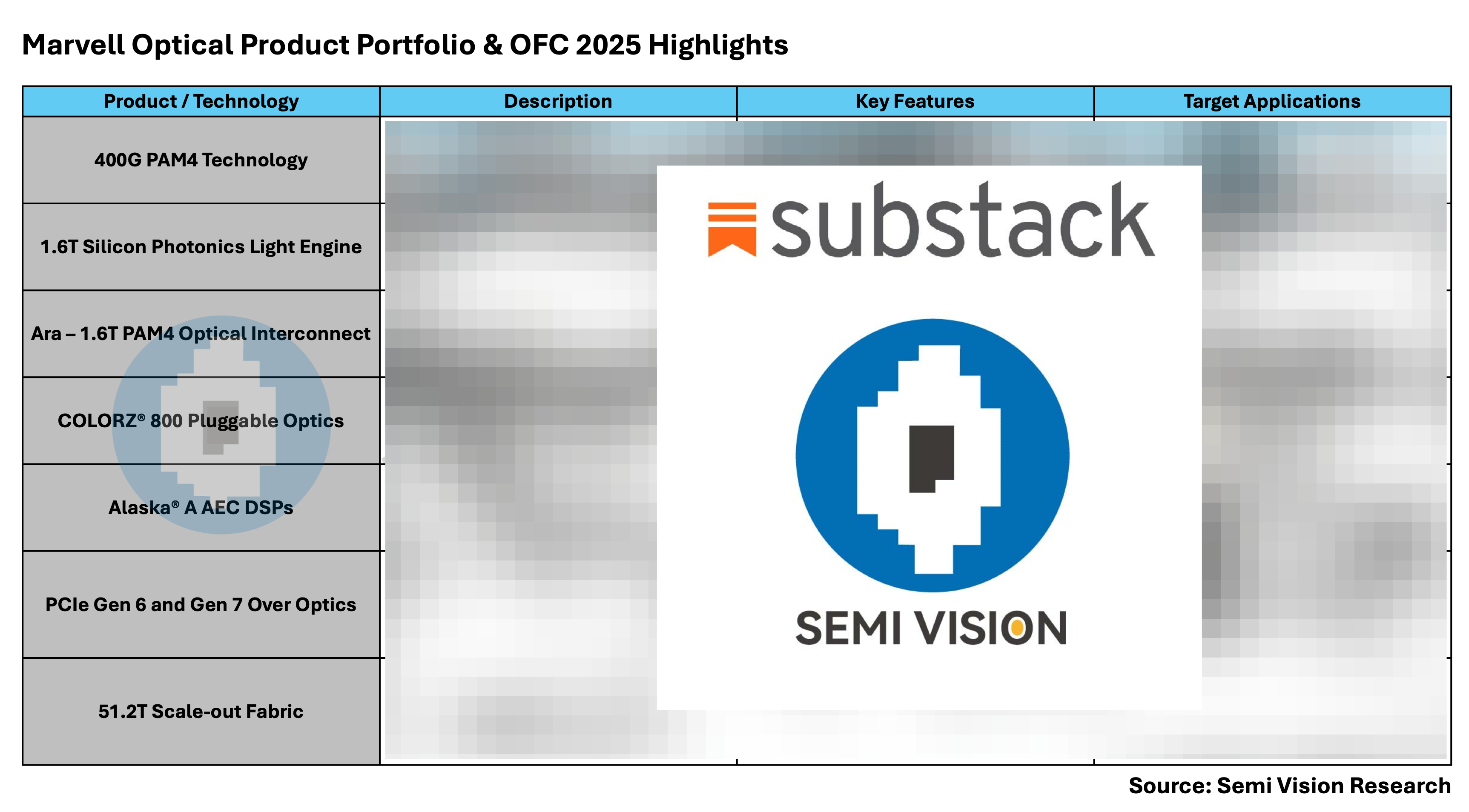
Marvell is actively expanding its efforts in the optical domain. We will provide a more in-depth exploration of Marvell’s silicon photonics developments in future discussions.
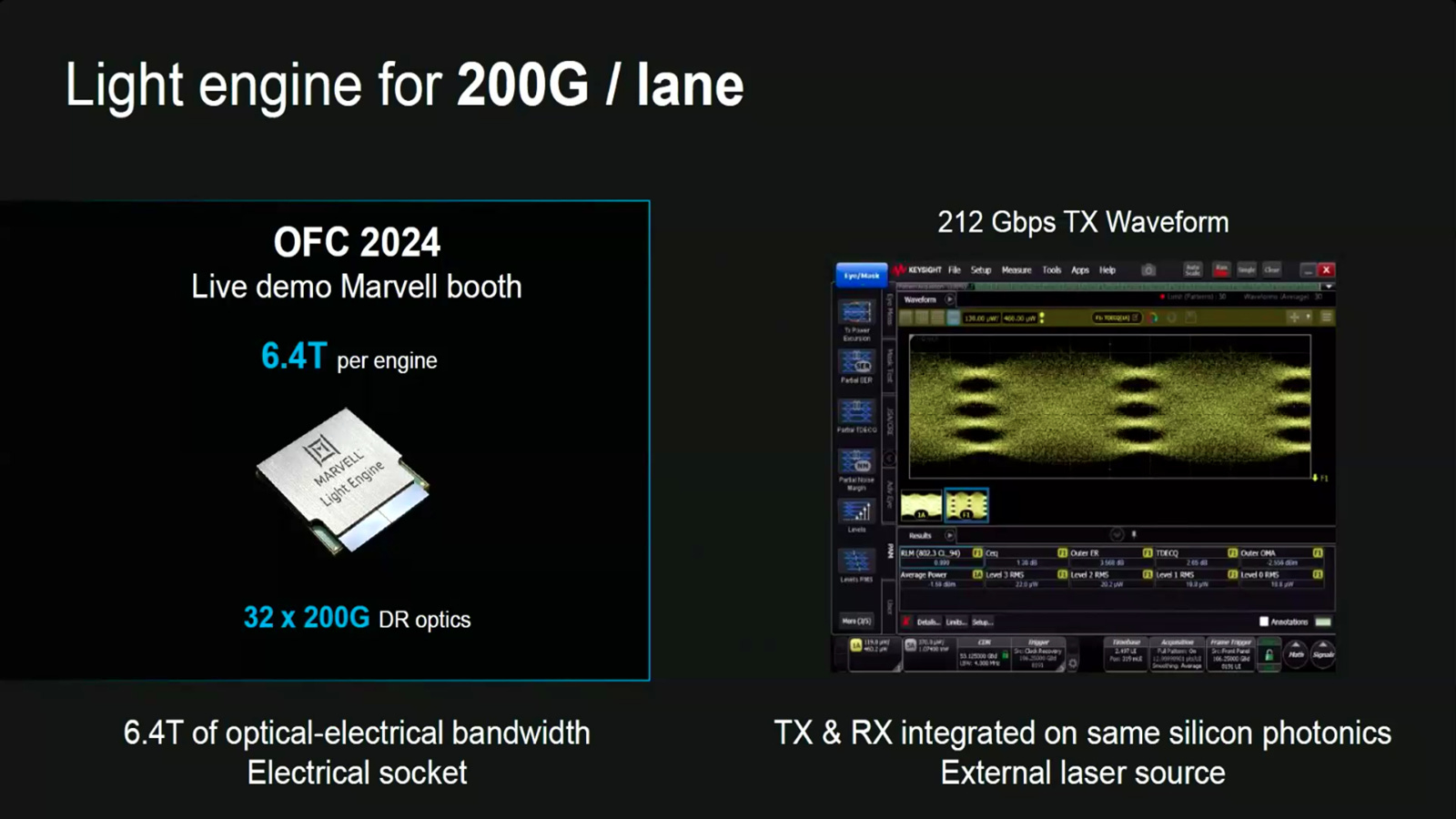
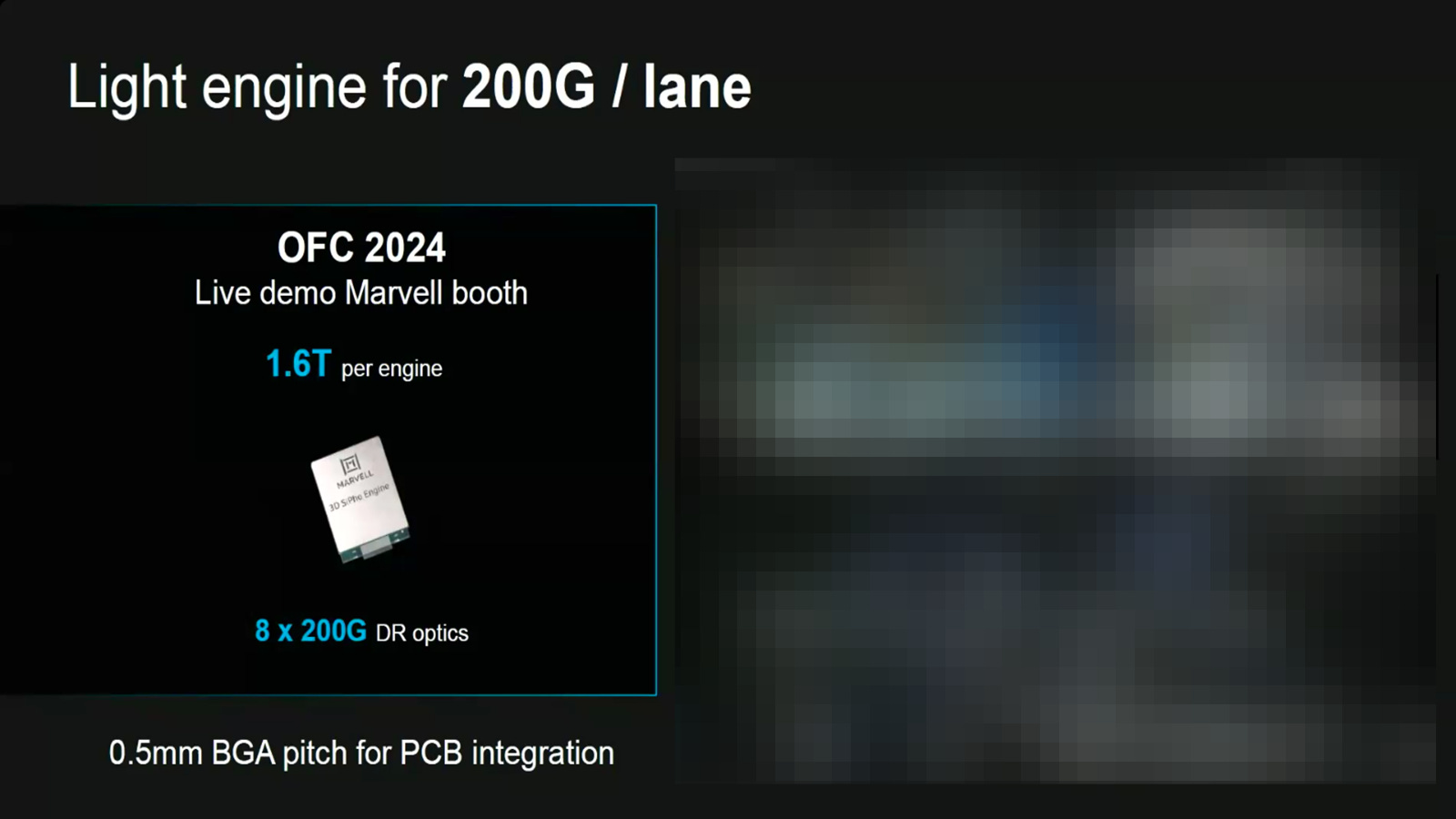
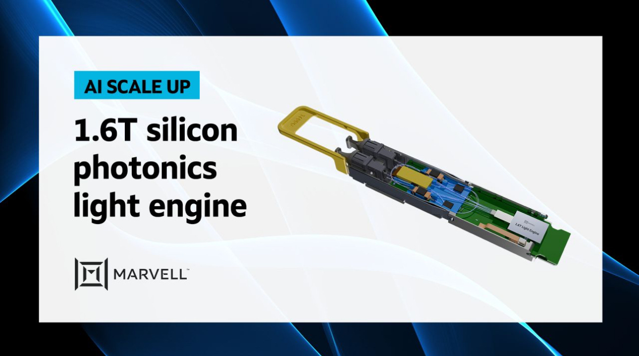
At OFC 2024, Marvell unveiled its 3D Silicon Photonics (SiPho) Engine, marking the industry’s first solution supporting 200Gbps electrical and optical interfaces. This technology serves as a foundational building block for integrating Co-Packaged Optics (CPO) directly into XPU-based architectures.
The Marvell 6.4T 3D SiPho Engine is a highly integrated optical engine featuring 32 channels of 200Gbps I/O — both electrical and optical — and incorporates hundreds of integrated components, including:
Silicon photonic components includes
• And a wide range of passive photonic components
Compared to legacy 100Gbps-class solutions, the engine delivers:
2× total bandwidth // 2× I/O bandwidth density // 30% lower energy per bit
Several major customers are currently evaluating the technology for integration into next-generation systems.
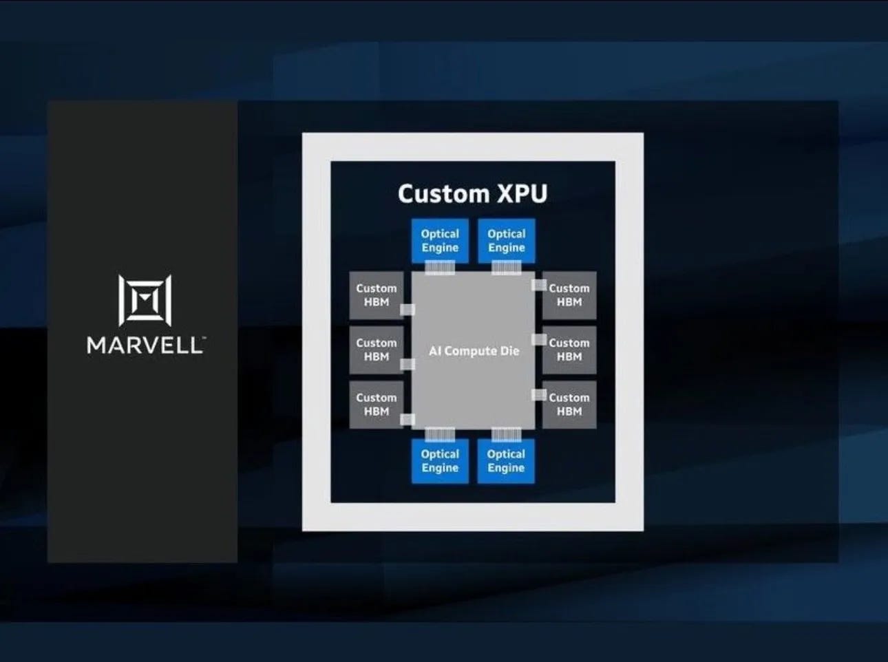
CPO and XPU Integration: Architecting Future AI Infrastructure
Marvell’s CPO strategy is central to its custom AI accelerator architecture, in which the XPU compute die, HBM stacks, and the 3D SiPho optical engine are co-packaged on a single substrate. This design leverages:
• High-speed SerDes
• Chip-to-chip optical interfaces
• Advanced packaging techniques
By embedding optics directly into the package, the solution eliminates the need for traditional electrical signaling across copper traces or cables, dramatically improving performance and efficiency. Optical I/O enables data transfers that are 100× faster and longer-reaching than electrical signals, while maintaining low latency and power consumption.
This architecture allows XPU clusters to scale across multiple racks, enabling disaggregated AI systems without compromising interconnect quality.
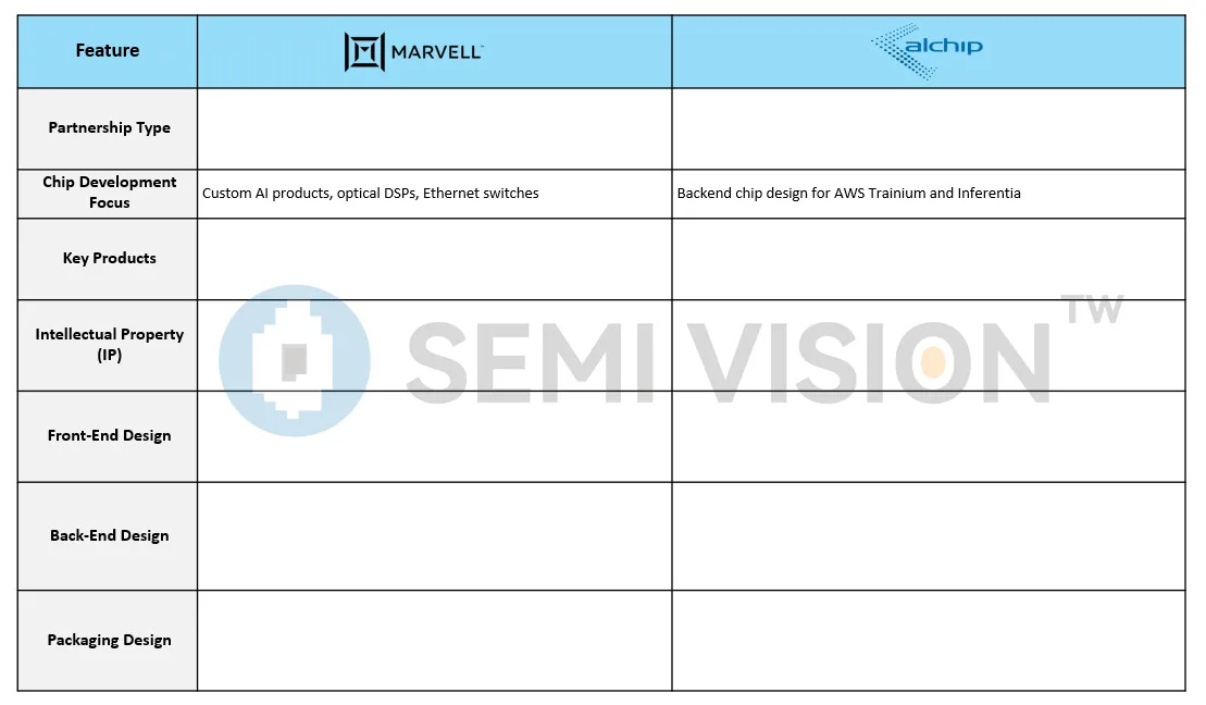
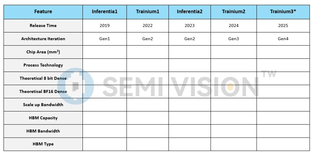
Marvell Business: A Giant in SerDes & Optical Interconnects
Marvell & AWS Collaboration: A Complex ASIC Partnership
CPO technology integrates optical components within a single tightly coupled package, significantly shortening electrical path lengths. Key benefits include:
• Reduced signal loss
• Enhanced signal integrity at high data rates
• Lower latency and jitter
• Improved energy efficiency, by reducing reliance on high-power drivers, retimers, and electrical repeaters
• Higher bandwidth density
• Greater resilience to electromagnetic interference (EMI)
These features make CPO an ideal enabler for high-performance, high-density, and scalable AI servers, optimized for next-gen accelerated compute infrastructure.
Marvell continues to propose forward-looking ideas in silicon photonics, shaping the direction of next-generation optical integration.
For more details, please refer to our earlier article on this topic.
TSMC’s Silicon Photonics Developments and Implications for NVIDIA
Key Findings from TSMC’s IEDM 2024 Research on Silicon Photonics
High-Performance Silicon Photonics Platform for Next-Gen Data Communications
CPO Packaging Solution
Detailed Discussion on NVIDIA’s Silicon Photonics Design
CPO Development statute updated (AMD (Ranovus), Broadcom, Cisco, IBM, Intel, and Marvell)
Silicon Photonics Manufacturing Process
CPO Process Flow
Photolithography to optical device (PIC)
Silicon Photonic Application
Evolution of Optical Communication in Data Centers and Bandwidth Demand
The Rise of Co-Packaged Optics (CPO)
Key Players’ CPO Developments
TSMC’s Integrated Optical Technologies (COUPE & CoWoS for Optics)
Taiwan’s Supply Chain Position in CPO Development
Development of Pluggable Optical Modules
Breakthroughs in Integrated Laser Source (ILS) Technology
Summary and Future Outlook(Nvidia Rubin chip)
Silicon Photonic Supply chain by SemiVision Research
Keep updated latest information to our Paid Members
TSMC Silicon Photonic Ecosystem
Nvidia Silicon Photonic Ecosystem
Taiwan Silicon Photonic Ecosystem
UMC Silicon Photonic Ecosystem
Global Silicon Photonic Ecosystem
Marvell Silicon Photonic Ecosystem
Broadcom Silicon Photonic Ecosystem
For Paid Members, SemiVision will provide the full tables and key keynote visuals from OFC 50 Conference
Skip the extension — just come straight here.
We’ve built a fast, permanent tool you can bookmark and use anytime.
Go To Paywall Unblock Tool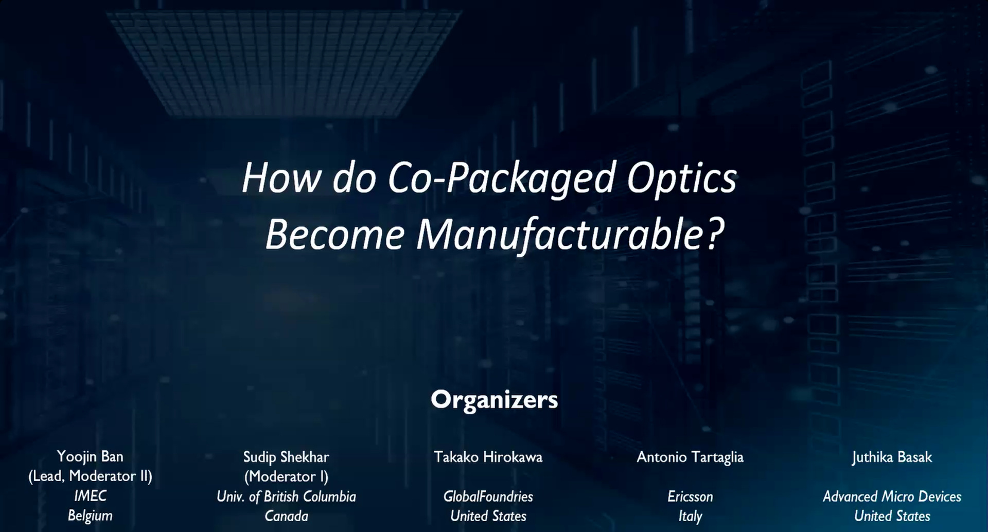